Virginia Polytechnic Institute and State University, along with NexGen Power Systems Inc in the USA, has announced the inaugural experimental characterization of dynamic on-resistance (RON) and threshold voltage (VTH) stability in vertical gallium nitride (GaN) power transistors, as reported by Xin Yang et al in the IEEE Transactions On Electron Devices, published online on December 5, 2023. The focus of the study involved NexGen junction field-effect transistor (JFET) devices with a voltage rating of up to 1200V (1.2kV).
Dynamic RON refers to the heightened resistance observed in switched transistors compared to the value in a steady DC state. The research team noted, "This issue can induce a higher conduction loss of the device and a degraded device lifetime in applications."
The researchers conducted a performance analysis, contrasting NexGen's 650V/200mΩ- and 1200V/70mΩ-rated GaN JFETs with commercial counterparts, including 650V and 1200V silicon carbide (SiC) metal-oxide-semiconductor FETs (MOSFETs, IMZA65R083M1H, C3M0075120D), and a 650V GaN high-electron-mobility transistor with Schottky-type p-GaN gate (SP-HEMT, GS-065-011-1-L).
NexGen's devices were manufactured on 100mm bulk n+-GaN substrates, featuring fin channels approximately 1μm high and sub-micron in width. The gate structure comprised implanted p-GaN regions situated between the fins. In the 650V and 1200V devices, the drift region between the fin channels and the drain measured around 8μm and 10μm, respectively. The corresponding estimated avalanche breakdown voltages were 800V and 1500V.
For the 1.2kV JFET, the threshold voltage (VTH) was recorded at 1.6V at 25°C, decreasing to 1.45V at 150°C. The on-resistance (RON) at a current of 20mA (IG) was approximately 70mΩ at 25°C, showing an increase to 150mΩ at 150°C.
The research employed continuous, hard switching double pulse tests (DPTs) with an active measurement circuit to evaluate the dynamic on-resistance (RON) performance. The devices were integrated into dual flat no-lead (DFN) packages, and the case temperature (TC) was determined through thermal imaging. While fan cooling was applied to the SiC MOSFET and GaN SP-HEMT comparison devices, it was not employed for the GaN JFETs. RON values were normalized based on the static RON at the measured TC.
The researchers noted, "The results demonstrate that 650V and 1200V GaN JFETs exhibit dynamic RON-free characteristics."
Additionally, static stress testing was conducted to assess the stability of RON and threshold voltage (VTH) values, particularly in scenarios where the power device is predominantly in an off state. For the 1200V JFET, the maximum VTH and RON shifts were determined to be 0.05% and 1.38%, respectively. In contrast, a 650V GaN SP-HEMT exhibited corresponding shifts on the order of 20% and 10%.
The researchers delved into simulations of JFET and HEMT structures to analyze the disparity in dynamic RON and static stability performance. They suggested a significant difference in the position of the peak electric field, with the HEMT structure having the peak field only 20-30nm from the device surface, while in the JFET, the peak electric field is buried about 1μm away from the surface. Coupled with lower defect density in epitaxial layers grown on bulk GaN, surface and buffer traps were largely suppressed, reducing delays in state changes and nearly eliminating dynamic RON in the GaN JFET.
The researchers added, "Finally, the native p-n junction gate in JFET has no band discontinuities, enabling more efficient carrier supply or extraction compared to the p-GaN/AlGaN/GaN hetero-gate in the HEMTs (particularly with the Schottky contact to p-GaN in SP-HEMT)."
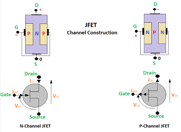
In an N channel JFET, the semiconductor material is of P type, and the substrate is N type. Conversely, in a P channel JFET, the semiconductor material is of N type, and the substrate utilized is P type. The JFET is constructed with a lengthy channel of semiconductor material, and ohmic contacts are established at both ends of the semiconductor channels to create source and drain connections. A P type JFET is characterized by numerous positive charges, while an N type JFET contains a substantial number of electrons.
JFET Operation
Water moves smoothly through a garden hose pipe in the absence of any obstruction, but when we gently compress the pipe, the water flow decelerates. This mirrors the operational principle of a Junction Field-Effect Transistor (JFET). In this analogy, the hose corresponds to the JFET, and the water flow represents the electric current. By configuring the current-carrying channel based on our requirements, we gain the ability to regulate the current flow.
When no voltage is applied across the source and gate, the channel serves as an unobstructed pathway for electrons to traverse. However, when a voltage polarity that reverses the P-N junction is applied, the channel constricts as the depletion layer expands. This adjustment can position the JFET in either the cut-off or pinch-off region.
JFET Types
Depending on the source of current flow, JFETs are classified into two types as follows:
n-channel JFET
p-channel JFET
The classification is based on whether the current flow is due to electrons or holes.
Junction Field Effect Transistor Applications
JFET is used as a switch
JFET is used as a chopper
JFET is used as a buffer
JFETs are used in oscillatory circuits
JFETs are used in cascade amplifiers
JFET Advantages
JFET has a high impedance
JFETs are low power consumption devices
JFET can be fabricated in a smaller size, and as a result, they occupy less space in circuits due to their smaller size.
JFET Disadvantages
It has a low gain-bandwidth product
The performance of JFET is affected as frequency increases due to feedback by internal capacitance.
Check out all of jfet junction field effect transistor options to find what you need and contact GUOYUAN ELECTRONICS for more imformation.

 Discrete Semiconductor Products
 Motors, Actuators, Solenoids and Drivers
 RF/IF and RFID
 Integrated Circuits (ICs)
 Inductors, Coils, Chokes
 English