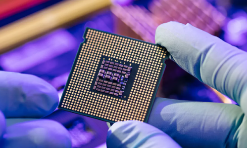
The Challenge in Semiconductor Development
Contemporary chips grapple with challenges related to cost, size, and energy consumption, rendering them less suitable for upcoming AI models in compact smart devices. Existing alternative approaches primarily target individual technical aspects such as energy efficiency, yet fall short in addressing the imperative need for cost reduction, accommodating the burgeoning size of AI models, and providing flexibility to support diverse classes of AI algorithms.
Moreover, the heavy reliance on major chip developers and manufacturers from the United States and China, such as Nvidia, TSMC, or Intel, underscores a significant dependency issue for the European technology sectors.
The current state of the semiconductor industry exposes a glaring lack of a compelling strategy for the future, inadequately meeting the demands of today's AI landscape.
The World'S Most Energy Efficient Semiconductors
Has achieved a significant milestone in advancing the world's most energy efficient semiconductor technology for AI inference. Named CapRAM™, this proprietary technology employs an innovative semiconductor device architecture utilizing a variable capacitor, known as a 'memcapacitor,' in contrast to conventional resistive approaches and transistors.
CapRAM™ minimizes electron movement, effectively reducing noise and resulting in a remarkable 20-fold increase in energy efficiency at the chip level. Beyond power consumption reduction, this breakthrough addresses a persistent challenge in processor technology by preventing overheating, allowing this chips to effectively utilize three dimensional space.
Within this spatial dimension, this German company employs a stacking approach, creating silicon dies or 'chiplets,' growing up to several hundred layers on a single substrate using in memory technology. This revolutionary design enables the support of AI models that are two to three hundred times larger than current capacities, with the potential for a 1000-fold expansion in the future.
Moreover, this technology harnesses conventional semiconductor materials, eliminating the need for extensive development processes in production. This not only enhances efficiency but also has the potential to save up to €100 million in development costs.
How Do Semiconductors Work?
The majority of semiconductors are constructed from crystals comprising various materials. To gain a deeper comprehension of semiconductor functioning, it is essential to grasp the nature of atoms and the organization of electrons within them. Electrons arrange themselves in layers known as shells within an atom, with the outermost layer termed the valence shell.
The electrons present in the valence shell are responsible for forming bonds with adjacent atoms, a phenomenon referred to as covalent bonds. Unlike most conductors, which typically possess just one electron in the valence shell, semiconductors typically have four electrons in their valence shell.
Nevertheless, if neighboring atoms share the same valence, electrons may establish bonds with the valence electrons of other atoms. This results in the self-organization of atoms into crystal structures. The majority of semiconductors are crafted using such crystals, with silicon crystals being particularly prominent in semiconductor production.
What is the Difference Between N Type and P Type Semiconductors?
An N type semiconductor predominantly conducts current through negatively charged electrons, akin to the flow of current in a wire. On the other hand, a P type semiconductor primarily carries current in the form of electron deficiencies known as holes, which possess a positive electric charge equal and opposite to that of an electron. In semiconductor materials, the movement of holes occurs in a direction contrary to the flow of electrons.
Elemental semiconductors encompass antimony, arsenic, boron, carbon, germanium, selenium, silicon, sulfur, and tellurium, with silicon being the most widely recognized, forming the foundation of most Integrated Circuits (ICs).
Additionally, common semiconductor compounds include gallium arsenide, indium antimonide, and oxides of various metals. Gallium arsenide (GaAs) is extensively employed in devices that amplify weak signals, offering low-noise and high-gain characteristics.
In comparison to the original vacuum tube, a semiconductor device can fulfill its function but in a significantly smaller form factor. A single Integrated Circuit (IC) has the capacity to execute tasks that would require a multitude of vacuum tubes, filling a large building and necessitating its own electricity generating facility, akin to a microprocessor chip.
What is a Semiconductor Chip?
A semiconductor material occupies the intermediate space between a conductor and an insulator, exercising control over the flow of electric current in electronic equipment and devices. This characteristic makes it a widely utilized component in electronic chips designed for computing elements and various electronic devices, including solid state storage.
What is an RF Semiconductor?
An RF (Radio Frequency) semiconductor serves as a component employed to activate or rectify power in electronic devices. Operating within the radio frequency spectrum, typically ranging from approximately 3KHz up to 300GHz, RF semiconductors play a crucial role in managing high frequency signals.
Check out all of general semiconductor diodes options to find what you need and contact GUOYUAN ELECTRONICS for more imformation.

 Discrete Semiconductor Products
 Motors, Actuators, Solenoids and Drivers
 RF/IF and RFID
 Integrated Circuits (ICs)
 Inductors, Coils, Chokes
 English